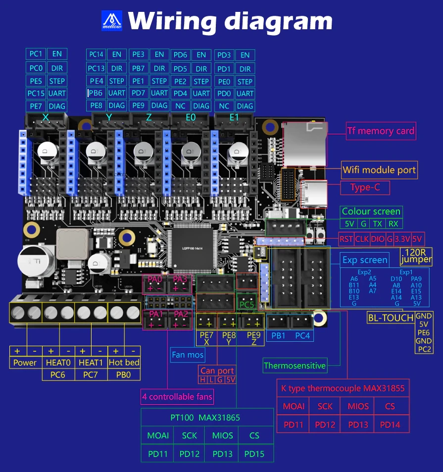
The pin names of the Fly-E3-v2
Edit me
Fly-E3-v2 Pinout Diagram
Important: The silk screen on the back of the Fly-E3-v2 has 4 errors. The EXP2 pin labeled A13 is Reset. The EXP2 pin labeled +5v is not connected. The Y driver socket STEP is PE4 and UART pin is PB6. The EXP1 pins labelled E14 and E15 are swapped. The diagrams below are correct.

Fly-E3-v2 Drivers Pins
Driver pin numbers. They are separated into driver number.
| Pin Type | 0 (X) | 1 (Y) | 2 (Z) | 3 (E0) | 4 (E1) | |
|---|---|---|---|---|---|---|
| Step Pins | PE_5 | PE_4 | PE_1 | PE_2 | PE_0 | |
| Direction Pins | PC_0 | PC_13 | PB_7 | PD_5 | PD_1 | |
| Enable Pins | PC_1 | PC_14 | PE_3 | PD_6 | PD_3 | |
| UART Pins | PC_15 | PB_6 | PD_7 | PD_4 | PD_0 |
Fly-E3-v2 Other Pins
If more than one pin name is availble, either name can be used in the firmware (config.g).
If the pins aren’t in the table (due to not having a special name), then the pin itself can be used in the form of PA0, PA.0, PA_0, A0, PA_0 or A_0.
| Pin Number | Pin Name 1 | Pin Name 2 |
|---|---|---|
| PC_4 | e0temp | t0 |
| PC_5 | e1temp | t1 |
| PB_1 | bedtemp | tb |
| PE_7 | xmin | xstop |
| PE_8 | ymin | ystop |
| PE_9 | zmin | zstop |
| PE_6 | servo0 | |
| PC_2 | probe | |
| PB_0 | bed | hbed |
| PC_6 | e0heat | he0 |
| PC_7 | e1heat | he1 |
| PA_0 | fan0 | fan |
| PA_1 | fan1 | |
| PA_2 | fan2 | |
| PA_3 | fan3 | |
| PD_10 | BEEP | |
| PA_8 | LCDEN | |
| PE_14 | LCDD5 | |
| PA_14 | LCDD6 | |
| PA_6 | LCDMISO | |
| PB_11 | BTNEN2 | |
| PB_10 | BTNEN1 | |
| PE_13 | TFCD | LCDCD |
| PC_9 | SDD1 | |
| PC_8 | SDD0 | |
| PC_12 | SDSCK | |
| PD_2 | SDCMD | |
| PC_11 | SDD3 | |
| PC_10 | SDD2 | |
| PA_9 | TX1 | BTNENC |
| PA_10 | RX1 | LCDRS |
| PE_15 | LCDD4 | |
| PA_13 | LCDD7 | |
| PA_5 | LCDSCK | |
| PA_4 | LCDSS | |
| PA_7 | LCDMOSI |